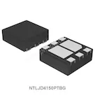
NTLJD4150PTBG數據表
![NTLJD4150PTBG數據表 頁面 1](http://pneda.ltd/static/datasheets/images/110/ntljd4150ptbg-0001.webp)
![NTLJD4150PTBG數據表 頁面 2](http://pneda.ltd/static/datasheets/images/110/ntljd4150ptbg-0002.webp)
![NTLJD4150PTBG數據表 頁面 3](http://pneda.ltd/static/datasheets/images/110/ntljd4150ptbg-0003.webp)
![NTLJD4150PTBG數據表 頁面 4](http://pneda.ltd/static/datasheets/images/110/ntljd4150ptbg-0004.webp)
![NTLJD4150PTBG數據表 頁面 5](http://pneda.ltd/static/datasheets/images/110/ntljd4150ptbg-0005.webp)
![NTLJD4150PTBG數據表 頁面 6](http://pneda.ltd/static/datasheets/images/110/ntljd4150ptbg-0006.webp)
![NTLJD4150PTBG數據表 頁面 7](http://pneda.ltd/static/datasheets/images/110/ntljd4150ptbg-0007.webp)
制造商 ON Semiconductor 系列 - FET類型 2 P-Channel (Dual) FET功能 Logic Level Gate 漏極至源極電壓(Vdss) 30V 電流-25°C時的連續漏極(Id) 1.8A Rds On(Max)@ Id,Vgs 135mOhm @ 4A, 10V Vgs(th)(最大)@ ID 2V @ 250µA 門電荷(Qg)(最大值)@ Vgs 4.5nC @ 4.5V 輸入電容(Ciss)(最大值)@ Vds 300pF @ 15V 功率-最大 700mW 工作溫度 -55°C ~ 150°C (TJ) 安裝類型 Surface Mount 包裝/箱 6-WDFN Exposed Pad 供應商設備包裝 6-WDFN (2x2) |